| Japanese | English |
15th LSI Design Contests・in Okinawa Design Specification - 4-1-1
4-1-1. FFT circuit : N=4
(1) Circuit design
Basic concept of 4 points FFT circuit which applies Radix-2 architecture is shown in figure 3.
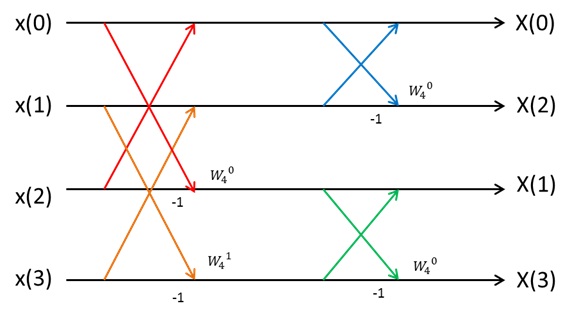
Figure 3: Basic concept of 4 points FFT circuit
In figure 3,4 point FFT circuit can implement by using 4 butterfly processing elements.
Block diagram is shown in figure 4.
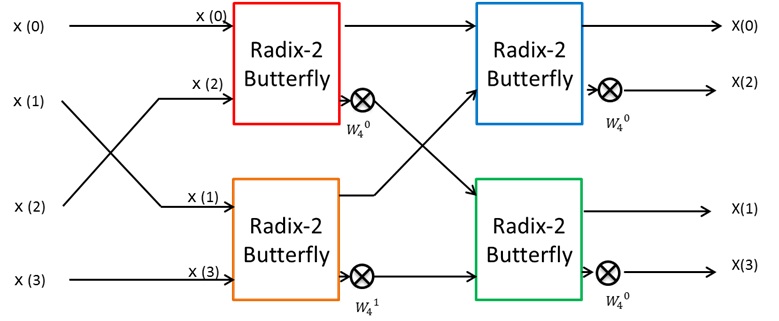
Figure 4: 4 points FFT circuit block diagram
In figure 3, butterfly processing element that is shown red line make be corresponding to red block in figure 4. Another butterfly processing element is same.
This is the 4 points FFT circuit for parallel input.
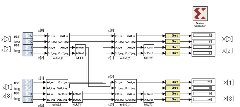
Figure 5: Design of 4 points FFT circuit for parallel input
The detail of each subsystem is shown below
a)radix2
In this part, we explain the Radix2_0, Radix2_1, Radix2_2 and Radix2_3 This circuit has 2 complex number inputs and 2 complex outputs. Therefore, real number and complex number must be separate input, and calculate each part. Architecture is shown figure 4.
Subsystem radix-2_1, radix-2_2, radix-2_3 is same as radix2_0.
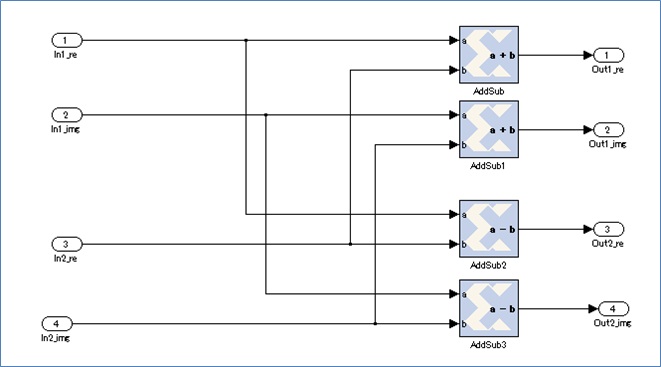
Figure 6: The model of subsystem radix-2_0
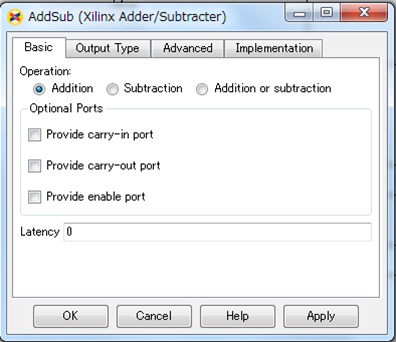
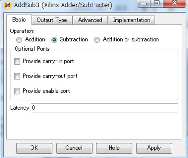
Figure 7: Parameter of AddSub Figure 8: Parameter of AddSub2
AddSub1 in figure 6 is same as AddSub.
AddSub3 is also same as AddSub2.
b) MULT
This section shows the MULT to the MULT3 subsystem.
The MULT subsystem multiplies a twiddle factor.
The Complex number operation ![]() mutiple
mutiple ![]() is showed by
is showed by 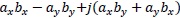
As following this process, multiple twiddle factors in terms of complex input. figure 9 shows the circuit block of the MULT subsystem. Abbreviate explanations of the MULT1 subsystem to the MULT3 subsystem, because of the same architecture as the MULT subsystem against the constant block, the W_real and the W_imag of figure 9, parameters.
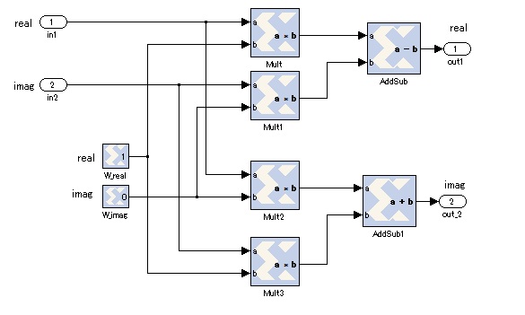
Figure 9: Architecture of the MULT subsystem
Abbreviate an explanation of the AddSub block, because of the same as the AddSub2 block of figure 6.
Also, abbreviate an explanation of the AddSub1 block, because of the same as the AddSub1 block of figure 6.
Figure 10 shows parameters of the Mult block.
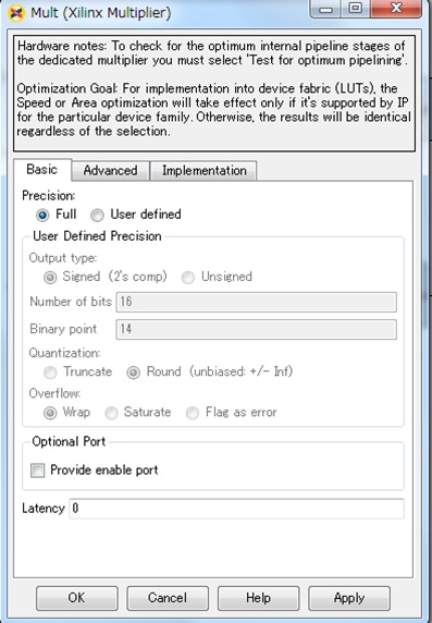
Abbreviate explanations of the Mult1 block, the Mult2 block and the Mult3 block, because of the same parameters as the Mult block of figure 9.
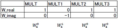
Table 1 shows the Constant block parameters showing the twiddle factors depending on ![]() or
or ![]() in the MULT subsystem, the MULT1 subsystem, the MULT2 subsystem and the MULT3 subsystem.
in the MULT subsystem, the MULT1 subsystem, the MULT2 subsystem and the MULT3 subsystem.
Table 1: Parameter of the twiddle factor
The subsystem MULT multiplies the complex twiddle factor in terms of the complex input signals.
(2) Verification
Input x[0] to x[3] of Table 2 into the FFT circuit of Fig.5, then got X[0] to X[3] of Table 2.
figure 11 shows the result of hardware simulation is consistent with the result of MATLAB simulation.
Table 2: Verification Result and Error on MATLAB
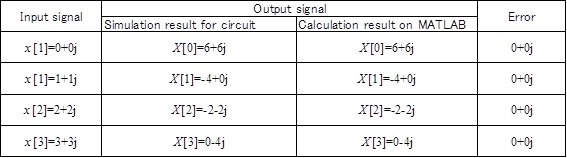
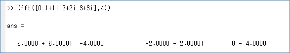
Figure 11: Calculation Result of FFT on MATLAB
Then, figure 12 and figure 13 shows the waveform of input signals and output signals.
Depending on this figure, in case of parallel input, FFT has no latency.
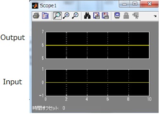
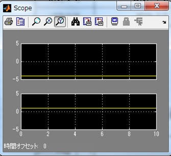
Figure 12: X[0]_real and x[0]_real Figure 13: X[1]_real and x[1]_real